

英伟达在去年的GTC 2022上发布了新一代基于Hopper架构的H100,用于下一代加速计算平台。其拥有800亿个晶体管,为CoWoS 2.5D晶圆级封装,单芯片设计,采用了台积电(TSMC)为英伟达量身定制的4N工艺制造。
目前英伟达提供了数种不同的H100计算卡,分别为H100 PCIe、H100 SXM和H100 NVL(双GPU版本)。其中普通的H100配备了80GB的HBM2E,PCIe和SXM5版本都有,H100 NVL则有着188GB的HBM3,对应每个GPU为94GB。近日更新的PCI ID列表显示,英伟达很快会为H100带来94GB和64GB的SXM版本,其中前者还会有针对中国市场的版本,型号为H800L 94GB。
64GB很好理解,但是94GB并不是寻常的数字,与H100 NVL的情况类似,英伟达并没有解释这种容量具体如何配置的。去年还有报道称,英伟达还准备了一款120GB的PCIe版本,不过至今还没有得到官方的确认,有可能只是在实验室测试的工程样品,最终不会出现在任何市场。
完整的GH100芯片配置了8组GPC、72组TPC、144组SM、共18432个FP32 CUDA核心,采用了第四代Tensor Core,共576个,并配有60MB的L2缓存。不过实际产品中没有全部打开,其中SXM5版本中启用了132组SM,共16896个FP32 CUDA核心,528个Tensor Core以及50MB的L2缓存,而PCIe 5.0版本则启用了114组SM,FP32 CUDA核心数量只有14592个。暂时不清楚拥有更大显存的H100的核心规格,估计会延续现有的配置。
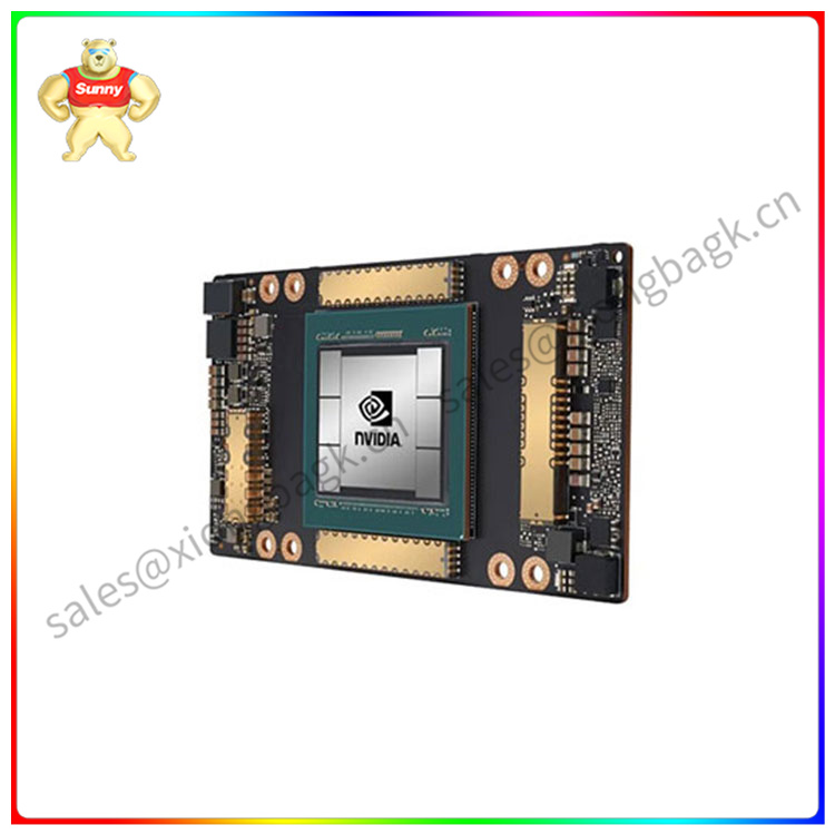
At last year's GTC 2022, Nvidia announced a new generation of H100 based on the Hopper architecture for the next generation of accelerated computing platform. It has 80 billion transistors in CoWoS 2.5D wafer-scale packaging, single-chip design, and is manufactured using a 4N process tailored for Nvidia by Taiwan Semiconductor Manufacturing Company (TSMC).
Nvidia currently offers several different H100 compute cards, namely H100 PCIe, H100 SXM, and H100 NVL (dual GPU version). The regular H100 comes with an 80GB HBM2E, available in both PCIe and SXM5 versions, and the H100 NVL comes with 188GB of HBM3, corresponding to 94GB per GPU. The recently updated PCI ID list shows that Nvidia will soon bring 94GB and 64GB SXM versions to the H100, with the former also having a version for the Chinese market, model H800L 94GB.
64GB is well understood, but 94GB is not a common number, and similar to the H100 NVL, Nvidia does not explain exactly how this capacity is configured. Last year, it was also reported that Nvidia was also preparing a 120GB PCIe version, but it has not been officially confirmed, and it is likely that it is just an engineering sample in a lab test and will not eventually appear in any market.
The complete GH100 chip is configured with 8 groups of GPC, 72 groups of TPC, 144 groups of SM, a total of 18,432 FP32 CUDA cores, using the fourth-generation Tensor Core, a total of 576, and equipped with 60MB L2 cache. However, not all of them are enabled in the actual product, among which the SXM5 version enables 132 SM, a total of 16,896 FP32 CUDA cores, 528 Tensor cores and 50MB L2 cache, while the PCIe 5.0 version enables 114 SM groups. There are only 14,592 CUDA cores in FP32. The core specifications of the H100 with larger memory are not yet known, and it is expected that the existing configuration will continue.