

英伟达 NVIDIA A100、A800、H100系列都有一些,未来的人工智能和算力产业基本都离不开这个产业和高端产品:
A100系列相信大家都比较熟悉,相比于英伟达前一代的 Volta GPU,A100 的性能提升了 20 倍,采用了英伟达的Ampere架构,拥有6912个CUDA核心和432个张量核心。它还配备了40GB、80GB或者160GB的高速HBM2显存,以及面向AI和机器学习的混合精度计算单元。非常适合于人工智能、数据分析、科学计算和云图形工作负载。芯片由 540 亿个组成,打包了第三代 Tensor 核心,并具有针对运算的加速功能,对于 AI 推理和训练来说特别有用。此外,每个 GPU 可以划分为多个实例,执行不同的推理任务,采用 Nvidia NVLink 互连技术可以将多个 A100 GPU 用于更大的 AI 推理工作负载。
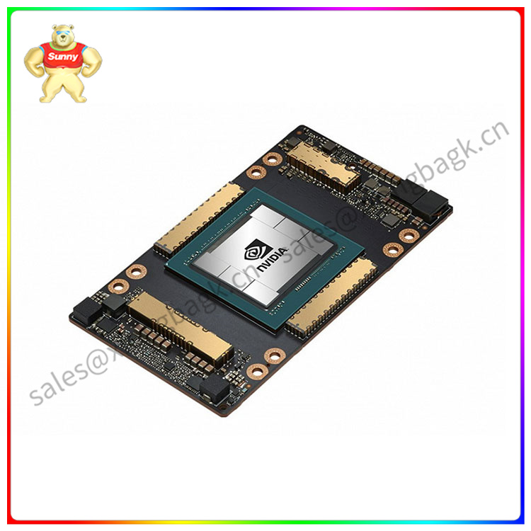
A800被视为是A100的,英伟达针对中国市场推出了特供芯片。A800计算性能与A100基本相同,但将NVLink高速互连总线的带宽从600GB/s降低到400GB/s。
至于H系列是目前主打的旗舰产品,未来都将会是H系列占主导,H100 是一款针对大模型专门优化过的芯片,使用台积电 5n制程(4N)打造,单块芯片包含 800 亿晶体管。同时也是全球首款 PCI-E 5 和 HBM 3 显卡,一块 H100 的 IO 带宽就是 40 terabyte 每秒。
NVIDIA A100, A800, H100 series have some, the future artificial intelligence and computing industry is basically inseparable from this industry and high-end products:
Compared to the previous generation of Nvidia Volta Gpus, the A100 improves performance by 20 times, uses Nvidia's Ampere architecture, and has 6912 CUDA cores and 432 tensor cores. It also comes with 40GB, 80GB or 160GB of high-speed HBM2 video memory and a mixed-precision computing unit for AI and machine learning. Ideal for AI, data analytics, scientific computing, and cloud graphics workloads. The chip, made up of 54 billion transistors, packs a third-generation Tensor core and has acceleration for sparse matrix operations, making it particularly useful for AI reasoning and training. In addition, each GPU can be divided into multiple instances to perform different inference tasks, and Nvidia NVLink interconnect technology allows multiple A100 Gpus to be used for larger AI inference workloads.
The A800 is seen as a "castrated version" of the A100, and Nvidia has launched a special chip for the Chinese market. The A800 has roughly the same computing performance as the A100, but reduces the bandwidth of the NVLink high-speed interconnect bus from 600GB/s to 400GB/s.
As for the H series is the current flagship product, the future will be dominated by the H series, H100 is a chip specifically optimized for large models, using TSMC 5nm custom version of the process (4N) to build, a single chip contains 80 billion transistors. It is also the world's first PCI-E 5 and HBM 3 graphics cards, and an H100 has an IO bandwidth of 40 terabyte per second.